INMOLD ELECTRONICS
Printed electronics is a technique that is an expansion moment, it is a printing method that allows you to create electronic devices on different kind of surfaces: thin, light and flexible.
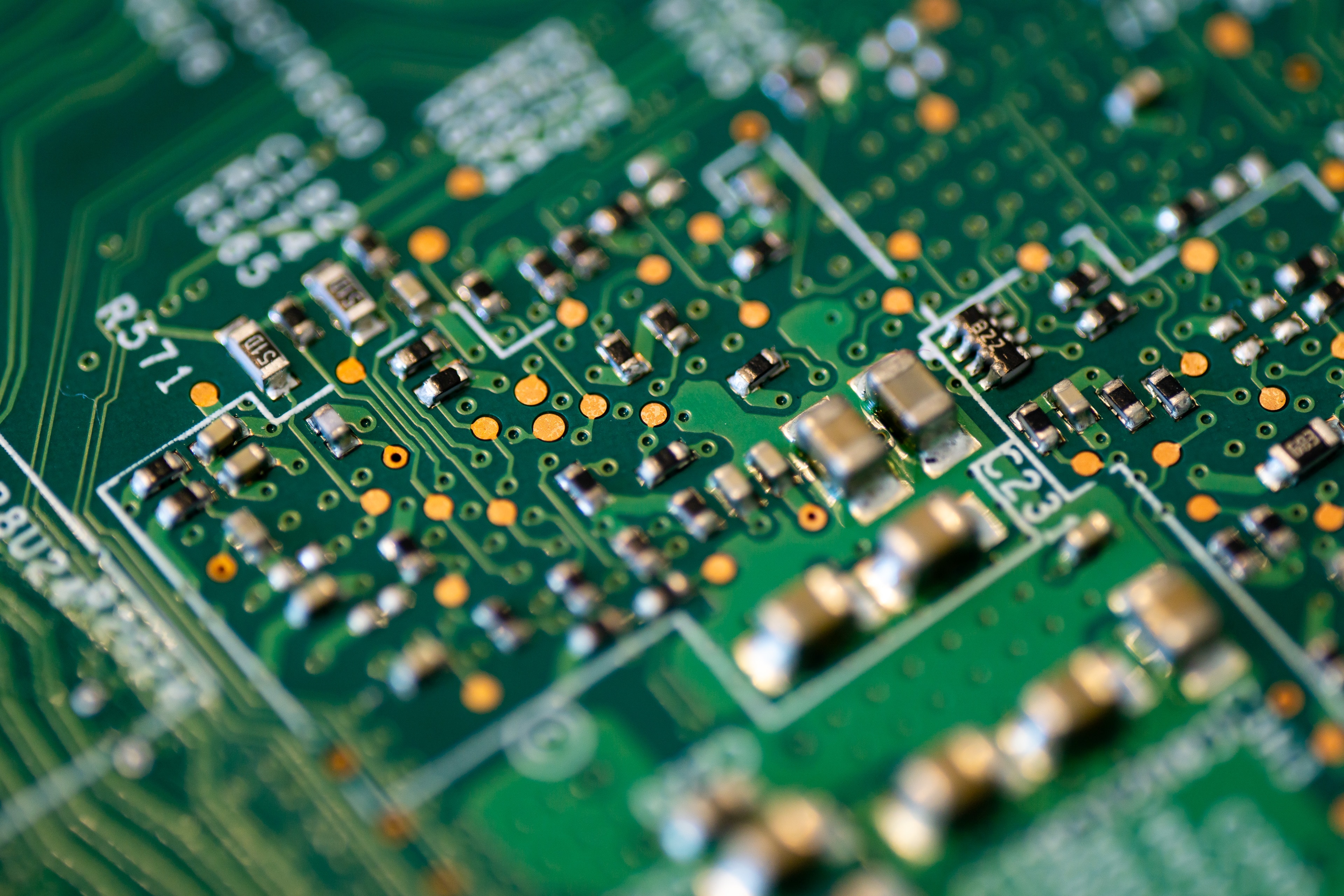
The creation of printed electronics consists of using communal printing equipment (screen printing, flexography, rotogravure, offset lithography and inkjet) to define the geometry, that is, the inks are formed by carbon force compounds and are deposited in layers. one on top of the substrate, it is dried at a temperature of about 120 ° C and subsequently the microcomponents are placed automatically.
This kind of electronics also associated with what is called inmold electronics. The procedure of printing the electronics in this system is the same as explained above, the main difference is that the substrate must be a polycarbonate or a deformable polyethylene and after applying heat to seal the ink the substrate must be shaped . This is done by high pressure or with vacuum.
WHERE IT IS APPLIED?
In these areas the applications of printed electronics are very varied:
- Accessories
- Automotion
- Aircraft
- Consumer electronics
More specifically we can find it in flexible and rolling screens, flexible photovoltaic cells, printed batteries, smart labels, smart packaging, RFID, posters, lighting, active clothing, car interiors…
This technique has numerous advantages such as lightness, space saving, robustness and freedom of design. In this way it allows designers to create new shapes and reduce materials and parts used, in addition to a significant reduction in weight, a factor that is often problematic in the manufacture of airplanes and helicopters.
Production is also benefited as thanks to this system, processing steps are reduced apart from the removal of bulky technology boxes.
As for the environment, it is also very important in reducing waste when printing electronics, in reducing lead use and thus complying with RoHS (Restriction of Hazardous Substances in electrical and electronic equipment).
In short, this technique is a breakthrough in terms of current electronics at all levels. It has a higher cost efficiency than traditional membrane switching panels, that is to say, that it is also relevant at an economic level since cost savings are beneficial for manufacturers.